As the bandwidth requirement increases Double Data Rate DDR interface is becoming very commonly used in many types of memories such as DDR IIIIII DRAM RLDRAM III QDR IIIII SRAM etc. DDR5 DDIMM uses OMI OpenCAPI Memory Interface as the host interface.
Understanding Ddr Ddr Protocol Truechip Vips
The DDR SDRAM uses DDR architecture to achieve high-speed operation.
. SSTL leverage s an active motherboard termination scheme and overcomes the signal integrity concerns with legacy LVTTL signaling. The newest members of the Fast Cycle RAM FCRAM series are 256 Mbit high-speed memories that incorporate the double data rate DDR SDRAM interface. 4 8 16 bit wide.
Commandsclock topology for high-speed operation in a high-loading condition September 30 2011 2011 Micron Technology Inc. The need for increasing speed higher memory size and power efficiency is driving the evolution in DDR and LPDDR interface technology as defined by JEDEC. DDR4 SDRAM operates at high data rate ie from 16Gbps to 32Gbps and the memory interface must be designed in a stringent way to comply with the specification set by JEDEC.
The major feature of DDR interface compared to a single data rate SDR one is to use both rising and falling edges of a clock to transfer data which allow it to provide two times the. The major feature of DDR interface compared to a single data rate SDR one is to. This tutorial provides overviews of recent advances in memory.
This webinar will provide a presentation on challenges and solutions associated with the development of high-speed interface design in modern SOCs. High speed Interface Design. Dynamic random-access memory SDRAM with a high bandwidth double data rate interface and has been in use since 2007It is the higher-speed successor to DDR and DDR2 and predecessor to DDR4 synchronous dynamic random.
Wi-FI module 1 lane Main Storage SSD 4 lanes Graphic card 16 lane DDR. Recent breakthroughs in semiconductor process technology allow for extreme high-speed interface designs which open the door to efficient chips with increased density. This is a significant data rate increase for DRAM modules over.
The design engineer can no longer simply connect data and address lines and expect to have a robust high-speed memory interface. 22 DDR Interface Design Considerations. Published in ASICON 11 December 2009.
Double data rate DDR4 3200 MTS source synchronous. Bandwidth for device memory. As the bandwidth requirement increases Double Data Rate DDR interface is becoming very commonly used in many types.
Double Data Rate 3 Synchronous Dynamic Random-Access Memory DDR3 SDRAM is a type of synchronous dynamic random-access memory SDRAM with a high bandwidth double data rate interface and has been in use since 2007It is the higher-speed successor to DDR and DDR2 and predecessor to DDR4 synchronous dynamic random-access memory SDRAM chips. Download Citation High speed DDR memory interface design form only given. DDR SDRAM Main Controller Block Before it is operational the DDR SDRAM memory.
Design verification and debugging - Compliance testing. DDR Memory Interface Design Considerations September 30 2011 2011 Micron Technology Inc. There are many technical issues to enhance the memory interface such as TSV interface high-speed serial interface including equalization ODT pre-emphasis wide IO interface including crosstalk skew cancellation and clock generation and distribution.
All the major challenges discussed in this paper have to be overcome for excellent signal integrity to guarantee minimum bit error rate in the multi-Gigabit transmission. Working closely with JEDEC Rohde Schwarz provides powerful solutions for DDR compliance testing. As the bandwidth requirement increases Double Data Rate DDR interface is becoming very commonly used in many types of memories such as DDR IIIIII DRAM RLDRAM III QDR IIIII SRAM etc.
High speed DDR memory interface design. The Cadence Denali DDR family of high-speed interface IP connects to external memories with the necessary bandwidth for applications. For DDR-I memories JEDEC created and adopted a low voltage high-speed signaling standard called series stub termination logic SSTL.
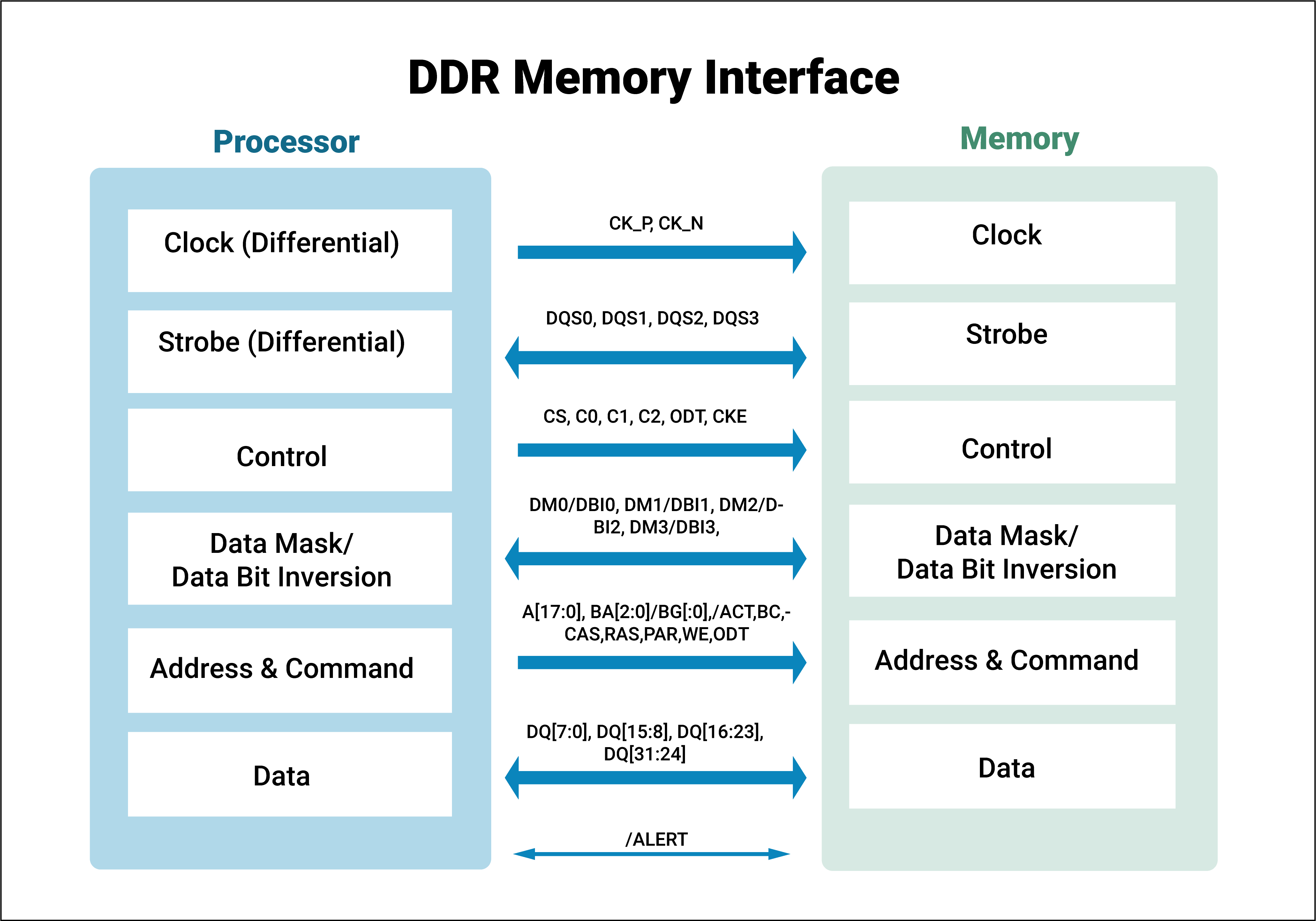
As part of the overall design DDR memory controller and memory. As the name implies SSTL is. The major feature of DDR interface compared to a single data rate SDR one is to use both rising and falling edges of a clock to transfer data which allow it to provide two times the throughput at the same clock frequencyThe high speed up to 16 GHz for DDR III nature and complex timing issues take the most attention for designers of ASIC chips with DDR memory controllers.
Summary form only given. On the DDIMM printed circuit board PCB the minimum data transfer rate per data differential pair over the OMI bus is 256Gbps. Memory bandwidth has been increased significantly.
Ad Authorized Distributor of Over 8 Million Electronic Components. High speed DDR memory interface design inproceedingsZhao2009HighSD titleHigh speed DDR memory interface design authorBrian Zhao booktitleASICON 2009 year2009 Brian Zhao. External double data rate DDR memory types are a common part of.
DDR5 Differential DIMM DDIMM is being defined in JEDEC and will be introduced to the market in 2020. The DDRAM is based on 2n pre-fetch architecture that can achieve two data words per clock pulse at the IO pins for a single read or write access. Common DDR memory parts are rated by column width eg.
Point to Point communication. The Denali High-Speed DDR PHY IP provides low latency and up to 4266Mbps throughput while balancing power consumption and minimizing area Developed by experienced teams with industry-leading. The major feature of DDR interface compared to a single data rate SDR one is to use both rising and falling edges of a clock to transfer data which allow it to provide two times the throughput at the same clock frequencyThe high speed up to 16 GHz for DDR III nature and complex timing issues take the most attention for designers of ASIC chips with DDR memory controllers.
Of a DDR design is the need to handle and pre-process strobe signals as opposed to generic clock signals. They are designed for high-performance. 985 MBps per lane PCIE V30 Gen 1.
High bus width typ. These techniques use IP to help gain an extra timing margin at high speed operation.

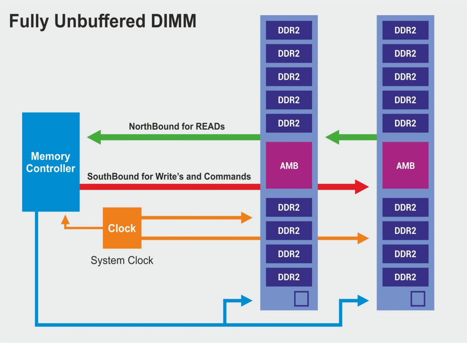
Ddr Memory Interface Basics 2017 07 05 Signal Integrity Journal

Ddr Phy Ip For Soc Designs Cadence Ip
Ddr Memory And The Challenges In Pcb Design Sierra Circuits

Ddr4 Phy Rambus
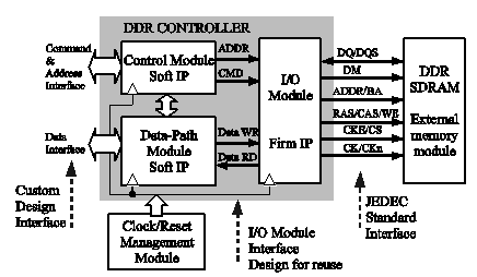
Ddr Sdram Controller Ip Designed For Reuse
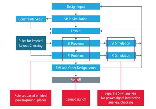
Implement Si And Pi In High Speed Memory Interfaces Signal And Power Integrity Pcb Ic Packaging Cadence Blogs Cadence Community

Ddr Controller Ip For Soc Designs Cadence Ip
2
0 comments
Post a Comment